
Deep tech on display: Scaleups and Corporates come together to spring innovation and business

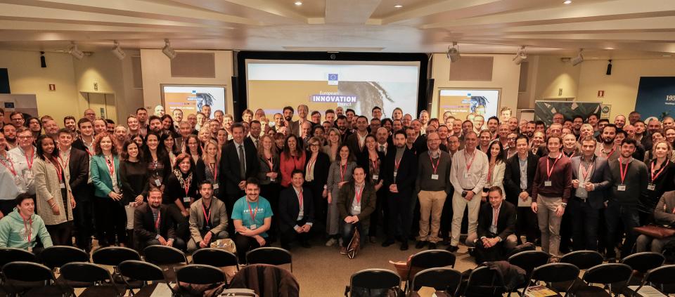
On 3-4 April, Nanografi was one of over 100 companies funded by the European Innovation Council (EIC) pilot that participated in a matchmaking event at the InQbet Accelerator in Brussels with large corporates and open innovation experts. Hosted by P&G and The Growcery, participants also included representatives from Cargill, Port of Antwerp, bpost, Nokia, Umicore, ING and Solvay and twenty other big corporations.
The event tackled important topics geared toward the scaleup community, including factors that influence corporate decisions when partnering with scaleups; the different ways corporates in different sectors approach open innovation; the importance of corporate innovation labs to fuel pilot projects and incubation; and important considerations scaleups should contemplate when partnering with larger corporations to push their products to market.
For the scaleups selected for the event, it was an important occasion to share their vision with an audience of experts and corporate insiders. A total of 103 entrepreneurs, coming from 25 European countries and Israel participated in 14 pitching sessions and more than 600 business meetings – a record figure the EIC Corporate Days.
We’re very happy to have participated in this event promoted by the EIC pilot. We hope the event will lead to positive follow ups and the ability to start a partnership that can help us scale-up our business.
The EIC Corporate Days link entrepreneurs with international companies to engage in open innovation towards new products, pilot projects and new business models. Since 2017, more than 400 companies funded under the EIC pilot programmes have participated in matchmaking events with large corporates across Europe.

Comments

Popular posts from this blog

Molybdenum Trioxide Nanoparticles/Nanopowder and Applications

General Information about Molybdenum Trioxide                                                     Molybdenum trioxide is chemical compound with the formula MoO3. Its chief application is as an oxidation catalyst and as a raw material for the production of molybdenum metal.  Molybdenum Trioxide  is a very light blue powder. Molybdenum Trioxide Nanoparticles/Nanopowder and Their Applications                                                    Like many  nanoparticles/nanopowder , Molybdenum Trioxide nanoparticles/nanopowder are used as catalysts. These catalysis reactions include hydrogenation catalysis and cracking catalysis. Molybdenum Trioxide nanoparticles/  nanopowder are useful for...

Improving Dialysis Process with Graphene

Researchers from Mechanical and Electrical Engineering Departments of MIT recently showed that graphene is a powerful material candidate for use in the dialysis systems (such as hemodialysis machines in medical institutes for filtering human blood). In order to prepare graphene as a dialysis material, researchers used a procedure opposite to the general treatments that nanotechnology people use. Dialysis is a process of filtering different solutions such as human blood by a membrane in order to remove waste molecules, drugs, chemical residues from the solution. In some cases, the process can be used for purification of chemicals or isolation of different molecules for medical diagnosis. It is an essential process for scientists especially in the medical operations. Image Retrieved From: http://www.graphene-nownano.manchester.ac.uk/our-research/examples-of-current-projects/fundamental-science/use-of-graphene-as-bio-membrane/ The traditional membranes used in dialysis are thick ...

Rundown about Silicon Oxide Wafer

The main insulating material used in micro-technology is Silicon Dioxide, which in chemical symbols is written as SiO2. In semiconductor technology, SiO2 thin film layers are mainly used as dielectric material film in transistors, capacitors (DRAM) or flash-memories. Silicon Oxide Wafers are produced using crystallization, solid state and other ultra-high purification processes such as sublimation. This process forms a cylindrical ingot, which is then sliced and polished to form wafers. Thermal oxide is a kind of "grown" oxide layer, compared to CVD deposited oxide layer, it has a higher uniformity, and higher dielectric strength, it is an excellent dielectric layer as an insulator . In most silicon- based devices, thermal oxide layer play an important role to pacify the silicon surface to act as doping barriers and as surface dielectrics. The simplest way to produce an insulating silicon oxide layers (SiO2) on silicon wafers is to oxidize silicon with oxygen, which ...