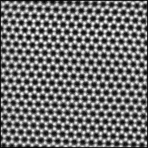
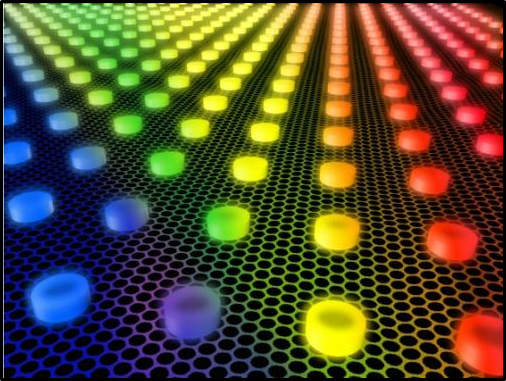
Graphene is a two-dimensional nanomaterial which is composed of monolayers of sp2-bounded carbon atoms. Graphene has drawn considerable attention in both academic and industry area for various potential applications including semiconductors, energy storage devices, and sensors due to their physical properties such as high room-temperature mobility and high thermal conductivity.
Find All Applications of Graphene Here: 60 Uses of Graphene – The Ultimate Guide to Graphene’s (Potential) Applications in 2019
Graphene's Photoresponsivity and Graphene Quantum Dots
Although graphene shows low photoresponsivity due to weak light absorption in its structure, there is an option to overcome this problem. Fortunately, Graphene Quantum Dots which are a type of graphene with lateral dimensions less than 100 nm, have unusual chemical, physical, electronical, optical properties from quantum confinement. Also, GQDs are considered to be an alternative to traditional fluorescent nanomaterials used in sensor applications. In addition, GQDs are environmentally friendly and promising green nanomaterials. Thus, combining the outstanding optical and electrical properties of GQDs with superior physical properties of graphene by forming hybrid structures, graphene-based UV sensors with performance can be constructed.
Why is it Important to Detect UV?
As it is well known that the detection of ultraviolet radiation has a great importance in both military and civilian fields such as optical communication, environmental monitoring, and others. In particular, UV monitoring is an important issue as UV radiation from the sun generates free-radical chemical species that cause various skin problems including aging and skin cancer. The combination of graphene-based hybrid materials can provide unique physical properties and show high photoresponsivity and detectivity.
Advantages of Graphene UV Sensors
Graphene-based UV sensors’ main advantage to other UV sensors is that they are flexible and transparent. Graphene UV sensors have remarkable transparency and superior mechanical flexibility without showing any significant change in electrical resistance. In addition, the synthesis of UV sensors is low-cost and executable.
To conclude, the discovery of graphene has stimulated a lot of research in numerous applications. Graphene and other two-dimensional materials have enabled a new class of materials to be developed. Even though graphene has limited responsivity, with chemical functionalization absorption can be enhanced and the responsivity can be improved. These improvements are achieved by combining graphene with other materials to form hybrid photodetectors. The improvements of interfaces between graphene and the other materials help to improve absorption coefficient. In summary, graphene-based photodetectors offer a small footprint promising for next-generation flexible and wearable electronics. The more investigations about graphene will help to develop more efficient devices used in various fields.
Comments
Post a Comment