
CVD Graphene

Graphene is a two-dimensional nanomaterial which is composed of monolayers of sp2-bounded carbon atoms. Graphene has drawn considerable attention in both academic and industry area for various potential applications including semiconductors, energy storage devices, and sensors due to their physical properties such as high room-temperature mobility, high thermal conductivity.
Obtaining single layer graphene or few-layer graphene by adhesive tape or cleavage methods is not practical because these methods provide only limited opportunity for scaling up the graphene. However, the chemical vapor deposition (CVD) process has been explored to synthesis large size single crystals and uniform films of monolayer graphene and bilayer graphene. CVD is a method to produce graphene which is fast, cheap and scalable. According to the experiences of graphene synthesis, it is well known that the growth of graphene is much easier from what is called ‘seed’.
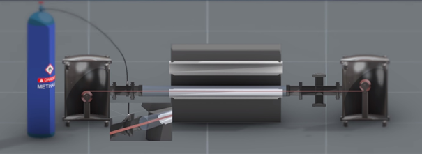
Chemical Vapor Deposition Process
CVD process is basically a method of depositing gaseous reactants onto a substrate. In CVD, pre-conditioned graphene (i.e. carbon nanotube, diamond) is scaled up by bombarding chemicals at high temperatures and pressures. The ‘seed’ (i.e. tiny pieces of actual diamond) is prepared for bombarding of chemicals. Then, high heat and pressure are applied, and chemical vapor deposit which contains carbon atoms (generally methane, CH4) is sprayed onto the seed. After some time (few days), grown graphene structure is obtained.
In CVD process there are several conditions which needs to be taken into consideration. In this prospect, the nucleation and growth mechanism of graphene on a catalytic substrate play the fundamental role in the formation of large domains and number of layers. The transition metals, alloys, and liquid metals have been recognized as the catalyst for growth of monolayer and bilayer graphene, where the surface composition of solid catalyst substrates also plays critical role on graphene growth. The thermodynamic and kinetic parameters are also crucial in graphene growth process, where pressure and temperature are both key factors.
 
To conclude, CVD is fast, cost-effective way of graphene production. Since by CVD, high quality graphene can be manufactured; it can be used in electronic applications such as creation of transistors and photovoltaic cells. In the future, CVD will be the most preferred method of synthesis of graphene.

Read more about this product:

Review of Chemical Vapor Deposition of Graphene

CVD Graphene - Monolayer Graphene on SiO2/Si Substrate

Nanografi's Horizon 2020 SME Instrument winner project: GREENGRAPHENE

Comments

Popular posts from this blog

Molybdenum Trioxide Nanoparticles/Nanopowder and Applications

General Information about Molybdenum Trioxide                                                     Molybdenum trioxide is chemical compound with the formula MoO3. Its chief application is as an oxidation catalyst and as a raw material for the production of molybdenum metal.  Molybdenum Trioxide  is a very light blue powder. Molybdenum Trioxide Nanoparticles/Nanopowder and Their Applications                                                    Like many  nanoparticles/nanopowder , Molybdenum Trioxide nanoparticles/nanopowder are used as catalysts. These catalysis reactions include hydrogenation catalysis and cracking catalysis. Molybdenum Trioxide nanoparticles/  nanopowder are useful for...

Improving Dialysis Process with Graphene

Researchers from Mechanical and Electrical Engineering Departments of MIT recently showed that graphene is a powerful material candidate for use in the dialysis systems (such as hemodialysis machines in medical institutes for filtering human blood). In order to prepare graphene as a dialysis material, researchers used a procedure opposite to the general treatments that nanotechnology people use. Dialysis is a process of filtering different solutions such as human blood by a membrane in order to remove waste molecules, drugs, chemical residues from the solution. In some cases, the process can be used for purification of chemicals or isolation of different molecules for medical diagnosis. It is an essential process for scientists especially in the medical operations. Image Retrieved From: http://www.graphene-nownano.manchester.ac.uk/our-research/examples-of-current-projects/fundamental-science/use-of-graphene-as-bio-membrane/ The traditional membranes used in dialysis are thick ...

Rundown about Silicon Oxide Wafer

The main insulating material used in micro-technology is Silicon Dioxide, which in chemical symbols is written as SiO2. In semiconductor technology, SiO2 thin film layers are mainly used as dielectric material film in transistors, capacitors (DRAM) or flash-memories. Silicon Oxide Wafers are produced using crystallization, solid state and other ultra-high purification processes such as sublimation. This process forms a cylindrical ingot, which is then sliced and polished to form wafers. Thermal oxide is a kind of "grown" oxide layer, compared to CVD deposited oxide layer, it has a higher uniformity, and higher dielectric strength, it is an excellent dielectric layer as an insulator . In most silicon- based devices, thermal oxide layer play an important role to pacify the silicon surface to act as doping barriers and as surface dielectrics. The simplest way to produce an insulating silicon oxide layers (SiO2) on silicon wafers is to oxidize silicon with oxygen, which ...