
Aluminum Nitride Sputtering Targets and Applications

Aluminum nitride is a chemical compound with the formula of AlN.
Aluminum nitride has excellent combination of physical, chemical, and mechanical properties. High-quality films of aluminum nitride have been used in various devices and sensors including the optical and optoelectronic devices. As far as the optical and optoelectronic applications are concerned, wide band gap (~6.2 eV) along with high-refractive index (~2.0) and low-absorption coefficient (<10−3) makes AlN a very attractive material for these applications. In addition to this, thermal and chemical stability of AlN films make it suitable for applications in difficult environment.
Today, AlN films/coatings have been grown by several methods which include pulsed laser deposition, reactive molecular beam epitaxy, vacuum arc/cathodic arc deposition, DC/RF reactive sputtering, ion beam sputtering, metal-organic chemical vapor deposition (MOCVD), and miscellaneous other techniques. Due to simplicity, reproducibility, ease of scaling up, and lower cost, magnetron sputtering is one of the common methods for growing AlN films for various applications.
Properties of AlN films depend upon the crystal structure, crystal orientation, microstructure, and chemical composition, which in turn depend upon the deposition conditions such as sputtering power, pulse frequency, duty cycle, growth temperature, nitrogen/argon flow ratio, and sputtering gas pressure. For detailed information you may click the link given below:
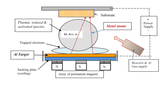
AlN sputtering targets give good result with the method of reactive DC magnetron sputtering system. You may see components of this system below.
For detailed information you may read the paper by clicking the link given below:
You may see our complete aluminum nitride sputtering target product range below.
TypeSizeThicknessPurityLink
Aluminum Nitride1'0.125''99.8%https://nanografi.com/sputtering-targets/aluminum-nitride-aln-sputtering-targets-size-1-thickness-0-125-purity-99-8/
Aluminum Nitride1'0.250''99.8%https://nanografi.com/sputtering-targets/aluminum-nitride-aln-sputtering-targets-size-1-thickness-0-250-purity-99-8/
Aluminum Nitride2'0.125''99.8%https://nanografi.com/sputtering-targets/aluminum-nitride-aln-sputtering-targets-size-2-thickness-0-125-purity-99-8/
Aluminum Nitride2'0.250''99.8%https://nanografi.com/sputtering-targets/aluminum-nitride-aln-sputtering-targets-size-2-thickness-0-250-purity-99-8/
Aluminum Nitride3'0.125''99.8%https://nanografi.com/sputtering-targets/aluminum-nitride-aln-sputtering-targets-size-3-thickness-0-125-purity-99-8/
Aluminum Nitride3'0.250''99.8%https://nanografi.com/sputtering-targets/aluminum-nitride-aln-sputtering-targets-size-3-thickness-0-250-purity-99-8/
Aluminum Nitride4'0.125''99.8%https://nanografi.com/sputtering-targets/aluminum-nitride-aln-sputtering-targets-size-4-thickness-0-125-purity-99-8/
Aluminum Nitride4'0.250''99.8%https://nanografi.com/sputtering-targets/aluminum-nitride-aln-sputtering-targets-size-4-thickness-0-250-purity-99-8/
Aluminum Nitride (Elastomer)1'0.125''99.8%https://nanografi.com/sputtering-targets/aluminum-nitride-elastomer-aln-sputtering-targets-size-1-thickness-0-125-purity-99-8/
Aluminum Nitride (Elastomer)2'0.125''99.8%https://nanografi.com/sputtering-targets/aluminum-nitride-elastomer-aln-sputtering-targets-size-2-thickness-0-125-purity-99-8/
Aluminum Nitride (Elastomer)3'0.125''99.8%https://nanografi.com/sputtering-targets/aluminum-nitride-elastomer-aln-sputtering-targets-size-3-thickness-0-125-purity-99-8/7

Comments

Popular posts from this blog

Molybdenum Trioxide Nanoparticles/Nanopowder and Applications

General Information about Molybdenum Trioxide                                                     Molybdenum trioxide is chemical compound with the formula MoO3. Its chief application is as an oxidation catalyst and as a raw material for the production of molybdenum metal.  Molybdenum Trioxide  is a very light blue powder. Molybdenum Trioxide Nanoparticles/Nanopowder and Their Applications                                                    Like many  nanoparticles/nanopowder , Molybdenum Trioxide nanoparticles/nanopowder are used as catalysts. These catalysis reactions include hydrogenation catalysis and cracking catalysis. Molybdenum Trioxide nanoparticles/  nanopowder are useful for...

Rundown about Silicon Oxide Wafer

The main insulating material used in micro-technology is Silicon Dioxide, which in chemical symbols is written as SiO2. In semiconductor technology, SiO2 thin film layers are mainly used as dielectric material film in transistors, capacitors (DRAM) or flash-memories. Silicon Oxide Wafers are produced using crystallization, solid state and other ultra-high purification processes such as sublimation. This process forms a cylindrical ingot, which is then sliced and polished to form wafers. Thermal oxide is a kind of "grown" oxide layer, compared to CVD deposited oxide layer, it has a higher uniformity, and higher dielectric strength, it is an excellent dielectric layer as an insulator . In most silicon- based devices, thermal oxide layer play an important role to pacify the silicon surface to act as doping barriers and as surface dielectrics. The simplest way to produce an insulating silicon oxide layers (SiO2) on silicon wafers is to oxidize silicon with oxygen, which ...

New Way of Deaf-Mute Communication with 3D Graphene

Image retrieved from: http://blogs.rsc.org/cc/2016/09/01/3d-graphene-adds-dimension-to-deaf%E2%80%93mute-communication/ Chinese scientists have developed wearable electronic device with conductive 3D graphene structure to translate sign language into written text. This technology can be applied by injecting graphene ink from a syringe under printed electronic field. For medical field, such as adhesive patches which determine heart, brain signal and neural activity, wearable and bio-integrated medical devices are very important. Due to noticeable properties of cast graphene, for example a 2D honeycomb lattice, excellent mechanical and electrical behaviors, Graphene has an important material in warble technology. However, it is difficult to preserve advantages of Graphene material in a 3D material which has an information about forces from every angle. Yanlin Song  and co-workers at the University of the Chinese Academy of Sciences, Beijing, and Shenyang Jianzhu University...