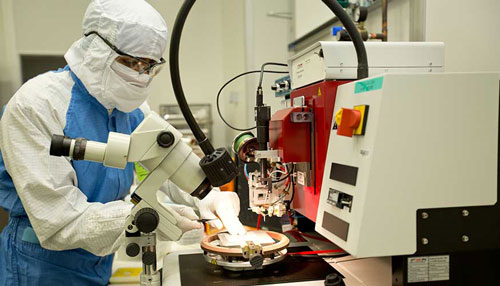
Image retrieved from : www.nanowerk.com
The nanotechnology started early with the National Nanotechnology Initiative (NION) initiated in 1986 by the UK National Physics Laboratory and DTI in Western Europe, where UK, Germany, France, Sweden and the Netherlands are particularly strong. First the nanotechnology institute was established and the "1998-2002 Foresight Program" announced nanotechnology as a strategic interest. Programs involving all of Europe, as well as national initiatives, have been put into effect. In the European Union, which was designated as the primary research area in October 2000, Nanotechnology allocated 82 million euros between 1998 and 2002 and 1.3 billion euros in the 6 th Framework Program covering 2002-2006. The large multinational companies of Europe, which make AR-GE in nanotechnology, Philips, Siemens, Bayer, Henkel, Degussa, Thompson CSF and Air Liquide.
NANOTECHNOLOGY IN USA
The "National Nanotechnology Initiative" which was approved by President Clinton in 2000 and launched on the offensive, attracted the attention of the world. Government support, which was $ 116 million in 1997, was approved at $ 270 million in 2000 and $ 422 million in 2001. In 2003, $ 710 million was foreseen for a budget of $ 520 million for 2002. Major companies active in nanotechnology include Dow Chemical, Mobil, Hewlett Packard, IBM, Chevvon, Dupont and others. The new look of NASA is "Nano-suited" and the model of this nanotechnology product is a cylinder 30 cm in diameter and 10 cm thick. In 2007, the planet is scheduled to be sent to the magnetosphere of the world to make detailed measurements of many nano-satellites. The American army is pursuing a new military uniform that makes the soldiers almost invisible, gives superhuman strength and provides immediate medical care. The task force is the famous Massachusetts Institute of Technology (MIT). The institute was awarded $ 50 million for 5 years for armor development, which can detect danger and protect against bullets and biological or chemical weapons. "We are not in the stage we want yet, but this is not a science fiction," says Ned Thomas, director of the MIT-affiliated Institute of Military Nanotechnology. All of this can be achieved by the development of nanoscale materials and devices called nanotechnology and their placement in uniform fabrics. "Supercharged shoes", soldiers can release the energy when they jump, and they can provide a 6-meter wall overrun. "Microreactors" can detect bleed and apply pressure. "Light deflector material" can make the appliance compatible with the environment. MIT research centers began working on nanotechnology ideas long before their collaboration with the military, but there was no military practice on their minds. However, Thomas said that there were bases for the progress of the revolution. Many nanotechnology institutes and centers have been opened in the US and the numbers are increasing rapidly. In addition, some universities have started to offer "Nanotechnology courses". Some of these increasingly numbered universities are Caltech, Harvard, MIT, NC State, Rice, USC and UC-Berkley.
Courses on nanotechnology have been reduced to the language level in the United States. Nanotechnology and nanotechnology, nanoparticle science and engineering, nano-scale manufacturing under the names of nanoscale processes, nanostructured materials and devices, nanotechnology, nanotechnology and engineering. In addition, the US National Science Foundation devoted $ 200 million to the National Science Foundation (NSF) nanotechnology undergraduate education in 2002 and has created training modules at various universities in Wisconsin, Cornell, Harvard, and Nothwestern. In the first place, these modules will be started in 10 places.
Posted by Şeyma KOÇ on February 21, 2017
Comments
Post a Comment