
n-doped and p-doped Silicon Sputtering Targets and Applications

Doping means the introduction of impurities into a semiconductor crystal to modify the conductivity. The two important elements that silicon can be doped with are boron and phosphorus.
The dopant is integrated into the lattice structure of silicon and the number of outer electrons define the type of doping. Elements with 3 valence electrons are used for p-type doping, in this case is boron; 5-valued elements for n-doping, in this case is phosphorus. By doping boron or phosphorus the conductivity of silicon can be increased.
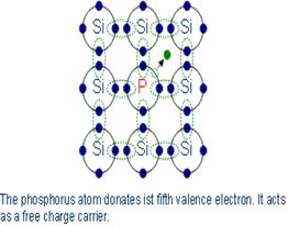
Phosphorus has an outer electron more than silicon. Four outer electrons combine with ever one silicon atom, while the fifth electron is free to move and serves as charge carrier. 
                                                            
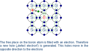
In contrast to the free electron due to doping with phosphorus, boron effect is exactly the opposite. Boron catches an additional outer electron, and leaves a hole in the valence band of silicon atoms. Therefore the electrons in the valence band become mobile.
                                                       
Now let's see the applications of n and p doped silicon sputtering targets. We can obviously say that silicon sputtering targets have many advantages. By silicon sputtering we can eliminate toxic gas release. Also the temperature of sputtering process for silicon is lower. Another advantage of silicon sputtering target is that we can control the amount of H2 incorporated in the deposited film.
When we look at the applications of silicon thin film we can see that in semiconductor electronics doped silicon films have a great importance. There are many methods to obtain doped silicon films like plasma enhanced chemical vapor deposition, hotwire chemical vapor deposition and magnetron sputtering. For these methods we can say that magnetron sputtering is an attractive technique in silicon thin film deposition. By magnetron sputtering of doped silicon you may obtain silicon thin film with higher carrier concentration and lower activation energy when we compare with undoped silicon.
If you need n or p doped silicon sputtering targets you may contact with us by clicking the links given below:

Comments

Popular posts from this blog

Molybdenum Trioxide Nanoparticles/Nanopowder and Applications

General Information about Molybdenum Trioxide                                                     Molybdenum trioxide is chemical compound with the formula MoO3. Its chief application is as an oxidation catalyst and as a raw material for the production of molybdenum metal.  Molybdenum Trioxide  is a very light blue powder. Molybdenum Trioxide Nanoparticles/Nanopowder and Their Applications                                                    Like many  nanoparticles/nanopowder , Molybdenum Trioxide nanoparticles/nanopowder are used as catalysts. These catalysis reactions include hydrogenation catalysis and cracking catalysis. Molybdenum Trioxide nanoparticles/  nanopowder are useful for...

Rundown about Silicon Oxide Wafer

The main insulating material used in micro-technology is Silicon Dioxide, which in chemical symbols is written as SiO2. In semiconductor technology, SiO2 thin film layers are mainly used as dielectric material film in transistors, capacitors (DRAM) or flash-memories. Silicon Oxide Wafers are produced using crystallization, solid state and other ultra-high purification processes such as sublimation. This process forms a cylindrical ingot, which is then sliced and polished to form wafers. Thermal oxide is a kind of "grown" oxide layer, compared to CVD deposited oxide layer, it has a higher uniformity, and higher dielectric strength, it is an excellent dielectric layer as an insulator . In most silicon- based devices, thermal oxide layer play an important role to pacify the silicon surface to act as doping barriers and as surface dielectrics. The simplest way to produce an insulating silicon oxide layers (SiO2) on silicon wafers is to oxidize silicon with oxygen, which ...

New Way of Deaf-Mute Communication with 3D Graphene

Image retrieved from: http://blogs.rsc.org/cc/2016/09/01/3d-graphene-adds-dimension-to-deaf%E2%80%93mute-communication/ Chinese scientists have developed wearable electronic device with conductive 3D graphene structure to translate sign language into written text. This technology can be applied by injecting graphene ink from a syringe under printed electronic field. For medical field, such as adhesive patches which determine heart, brain signal and neural activity, wearable and bio-integrated medical devices are very important. Due to noticeable properties of cast graphene, for example a 2D honeycomb lattice, excellent mechanical and electrical behaviors, Graphene has an important material in warble technology. However, it is difficult to preserve advantages of Graphene material in a 3D material which has an information about forces from every angle. Yanlin Song  and co-workers at the University of the Chinese Academy of Sciences, Beijing, and Shenyang Jianzhu University...