
Silicon Nitride Wafer Applications

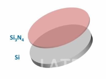
Silicon Nitride Coating - stoichiometric trisilicon tetranitride (Si3N4) thanks to its very high mechanical and thermal stability is used for tools such as roller bearings used under harsh conditions. In the semiconductor industry, silicon nitride layers are used as dielectric material, passivation layers or can act as hardmask mask. Silicon Nitride has good high temperature strength, creep resistance and oxidation resistance. Silicon Nitride's low thermal expansion coefficient gives good thermal shock resistance. Silicon Nitride is produced in three main types; Reaction Bonded Silicon Nitride (RBSN), Hot Pressed Silicon Nitride (HPSN) and Sintered Silicon Nitride (SSN).
There are two main depositions of silicon nitride layers:
LPCVD Silicon Nitride – Low pressure chemical vapor deposition silicon nitride. LPCVD silicon nitride layers are easily deposited on silicon wafers in a reproducible, pure and uniform way. This leads to silicon nitride layers with low electrical conductivity, very good coverage of edges and high thermal stability. SiNx layers realized by the low pressure chemical vapour deposition (LPCVD) technique typically shows a lower H-content and higher stability against HF.
PECVD Silicon Nitride - plasma enhanced chemical vapour deposition silicon nitride.PECVD silicon nitride layers allow higher growth rate, which therefore leads to thicker layers. Stoichiometry and stress can also be adjusted. High thickness uniformity and etch rates are eventually obtained. PECVD Silicon nitride wafers are particularly suitable for passivation layers. SiNx layers realized by the plasma enhanced chemical vapour deposition (PECVD) technique from SiH4 and NH3 typically – depending on the deposition temperature and gas composition – contain 5 - 20 atom% hydrogen which saturates dangling bonds and thus chemically and mechanically stabilizes the SiNx lattice.
For semiconductor devices, the chemical, electrical and optical properties of amorphous hydrogenated silicon nitride (SiNx) make this material well-suited for different applications, such as for
  • ­passivation or insulating layers in integrated circuits
  • ­masking or etch stop material in wet and plasma etching processes due to its high chemical stability
  • ­masking material in silicon oxidation processes due to the very low oxygen diffusion coefficient in SiNx
  • ­anti-reflective coating in photovoltaics due to its adjustable refractive index
  • Another applications:
  • ­Silicon Nitride (SiNx) wafers are used in MEMS devices
  • ­Silicon Nitride (SiNx) wafers are used in Passivation/Barrier film
  • ­Silicon Nitride (SiNx) wafers are used in Integrated circuits (IC)
  • ­Silicon Nitride (SiNx) wafers are used in Hard mask for wet and dry etching
  • ­Silicon Nitride (SiNx) wafers are used in Micro-mechanics.

Comments

Popular posts from this blog

Molybdenum Trioxide Nanoparticles/Nanopowder and Applications

General Information about Molybdenum Trioxide                                                     Molybdenum trioxide is chemical compound with the formula MoO3. Its chief application is as an oxidation catalyst and as a raw material for the production of molybdenum metal.  Molybdenum Trioxide  is a very light blue powder. Molybdenum Trioxide Nanoparticles/Nanopowder and Their Applications                                                    Like many  nanoparticles/nanopowder , Molybdenum Trioxide nanoparticles/nanopowder are used as catalysts. These catalysis reactions include hydrogenation catalysis and cracking catalysis. Molybdenum Trioxide nanoparticles/  nanopowder are useful for...

Rundown about Silicon Oxide Wafer

The main insulating material used in micro-technology is Silicon Dioxide, which in chemical symbols is written as SiO2. In semiconductor technology, SiO2 thin film layers are mainly used as dielectric material film in transistors, capacitors (DRAM) or flash-memories. Silicon Oxide Wafers are produced using crystallization, solid state and other ultra-high purification processes such as sublimation. This process forms a cylindrical ingot, which is then sliced and polished to form wafers. Thermal oxide is a kind of "grown" oxide layer, compared to CVD deposited oxide layer, it has a higher uniformity, and higher dielectric strength, it is an excellent dielectric layer as an insulator . In most silicon- based devices, thermal oxide layer play an important role to pacify the silicon surface to act as doping barriers and as surface dielectrics. The simplest way to produce an insulating silicon oxide layers (SiO2) on silicon wafers is to oxidize silicon with oxygen, which ...

Hydroxyapatite Nanopowders and Their Applications

Hydroxyapatite, is a naturally occurring mineral form of calcium apatite with the formula Ca 5 (PO 4 ) 3 (OH). Pure hydroxyapatite powder is white. Naturally occurring apatites can, however, also have brown, yellow, or green colorations, comparable to the discolorations of dental fluorosis. Hydroxyapatite Nanopowder/Nanoparticles (50 nm, 99.95+%)  has been widely used as a biocompatible ceramic in many areas of medicine, but mainly for contact with bone tissue, due to its resemblance to mineral bone. In mammals, the skeleton presents a carbonated and partially substituted apatite, based on nanocrystal aggregates, and associated with collagen, building up 3-D structures present in various bone tissue conformations like trabecular or cancellous bone. There has been growing interest in developing bioactive synthetic ceramics that could closely mimic natural apatite characteristics. As mentioned before,  Hydroxyapatite Nanopowder  is the main inorganic constituent of bon...