
Rundown about Silicon Oxide Wafer

The main insulating material used in micro-technology is Silicon Dioxide, which in chemical symbols is written as SiO2. In semiconductor technology, SiO2 thin film layers are mainly used as dielectric material film in transistors, capacitors (DRAM) or flash-memories.
Silicon Oxide Wafers are produced using crystallization, solid state and other ultra-high purification processes such as sublimation. This process forms a cylindrical ingot, which is then sliced and polished to form wafers.
Thermal oxide is a kind of "grown" oxide layer, compared to CVD deposited oxide layer, it has a higher uniformity, and higher dielectric strength, it is an excellent dielectric layer as an insulator . In most silicon- based devices, thermal oxide layer play an important role to pacify the silicon surface to act as doping barriers and as surface dielectrics.
The simplest way to produce an insulating silicon oxide layers (SiO2) on silicon wafers is to oxidize silicon with oxygen, which can be carried out via high dry or wet oxidation processes. In both cases, silicon reacts with oxygen leading to a moving interface towards the substrate. Thermal oxide is normally grown in a horizontal tube furnace
Dry oxidation typically takes place at temperatures in between 850 and 1200°C and it demonstrates low growth rates. It does allow very good thickness uniformity and purity. Therefore, this is the preferred way to produce high quality thin silicon oxide layers. Thicker oxide layers are typically produced by wet oxidation where the growth rate is significantly increased.
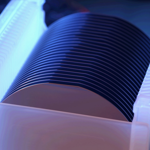
Applications of Silicon Oxide (SiO2) wafers:
- Silicon Oxide (SiO2) wafers are used as dielectric material.
- Silicon Oxide (SiO2) wafers are used in Micro Electro Mechanical Systems (MEMS) devices.
- Silicon Oxide (SiO2) wafers are used as an antireflection layer on e.g. solar cells.
- Silicon Oxide (SiO2) wafers are used as a hard mask for diffusion.
- Silicon Oxide (SiO2) wafers are used for wet or dry chemical etching
- Silicon Oxide (SiO2) wafers are used as an isolator between integrated devices.

Comments

Popular posts from this blog

Molybdenum Trioxide Nanoparticles/Nanopowder and Applications

General Information about Molybdenum Trioxide                                                     Molybdenum trioxide is chemical compound with the formula MoO3. Its chief application is as an oxidation catalyst and as a raw material for the production of molybdenum metal.  Molybdenum Trioxide  is a very light blue powder. Molybdenum Trioxide Nanoparticles/Nanopowder and Their Applications                                                    Like many  nanoparticles/nanopowder , Molybdenum Trioxide nanoparticles/nanopowder are used as catalysts. These catalysis reactions include hydrogenation catalysis and cracking catalysis. Molybdenum Trioxide nanoparticles/  nanopowder are useful for...

Titanium Carbide Powders and Applications

Titanium carbide which has the chemical formula of TiC attracted great interest for many structural applications due to its extremely high melting temperature, high hardness, high chemical resistance and good electrical conductivity. Therefore titanium carbide can be used in cutting tools, grinding wheels, wear-resistant coatings, high temperature heat exchangers, magnetic recording heads, turbine engine seals, and bullet-proof vests, etc. In addition, a promising field of application comprises plasma and flame spraying processes in air, where titanium carbide-based powders show high-phase stability. TiC(Titanium Carbide Powder) (325 mesh, 99,9+%)  can also be used in biomedical implant devices. Materials used for biomedical implant devices must satisfy a variety of property demands, which are often mutually exclusive. Further, different parts of a device demand different material properties. These factors often make it difficult to manufacture a medical device using a...

Bismuth Oxide Sputtering Targets and Applications

Bismuth oxide with the chemical formula of Bi 2 O 3  is one the most important bismuth compounds. Bismuth oxide has been investigated extensively due to its optical and electrical properties such as large energy gap (from 2 to 4 eV), refractive index and high oxygen ion conductivity at high and medium temperatures. These properties make bismuth oxide one of the most perspective candidates for application in optoelectronics, solar cells and solid oxide fuel cells (SOFCs). Bismuth oxide has a few main polymorphic forms that are known as α, β, γ, δ. All polymorphs have different crystal structure and various optical, electrical and mechanical properties. Only two of them, the low temperature monoclinic α-phase and high temperature face-centered cubic δ-phase are stable. The other phases are metastable. Magnetron sputtering is a widespread method because of high deposition rate, dense and highly adhesive films, and possibility of using commercially available large area depositio...