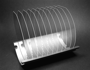
Fused Silica Wafers are thin, circular pieces of UV fused silica originally designed for the use as test substrates to measure the quality of optical coatings. Fused Silica also sometimes called “Fused Quartz” is the amorphous phase (glassy form) of quartz (SiO2) and is thus isotropic. It is tough and hard and has a very low expansion. It has no additives, unlike e.g. borosilicate glass, thus is pure SiO2. Fused silica has higher transmission in the ultraviolet and infrared spectrum, a superior chemical resistance and high dielectric strength, a very low thermal expansion coefficient and a high softening point and high thermal resistance. Standard thicknesses of fused silica wafers are 500, 700 and 1000 μm with diameters of 2, 3, 4 and 6 inches.
Production process of fused silica mainly consists of the method of melting and re-solidifying of ultrapure SiO2. Silicon-rich chemical precursors such as SiCl4 are used for synthesis of fused silica by the process of gasifying and oxidizing in a H2+O2 atmosphere. The SiO2 dust formed during that process is fused to silica on a substrate. This method offers a better optical transmission in the deep ultraviolet. The fused silica blocks are sliced and polished from both sides, then, the wafers are ultrasonically cleaned and stored in contaminant-free packaging.
There are different types Fused Silica used for different applications.
Ultraviolet Grade Fused Silica - JGS1
JGS1 is transparent in the ultraviolet and visible regions. It has no absorption bands in 170-250 nm wavelength intervals. The transmission in the VIS and UV (down to approx. 215 nm) is approx. 90 % (only reflection losses) and drops between 215 and 150 nm down to 0 %. In the infrared range, the comparable high OH-concentration of typically 1000 ppm causes absorption bands for wavelengths > 1.2 μm and has intensive OH absorption band in the interval of wavelength 2600-2800 nm. JGS1 is used for optics operating in the deep UV and the visible wavelength range (Laser Lenses, Windows, Prisms, Mirrors, etc.). It is practically free of bubbles and inclusions.
Optical Grade Fused Quartz - JGS2
Compared to JGS1 wafers, the transmission range of the cheaper JGS2 wafers is shifted towards longer wavelengths: UV-absorption already starts below approx. 270 nm wavelength, while in the VIS and IR the transmission is approx. 90 % up to approx. 2 μm wavelength due to the lower OH-concentration (typ. < 300 ppm). JGS2 wafers can be made in small diameters/dimensions that can be very thin and is free of bubbles. Cons include possible bubbles in larger dimensions/diameters. Applications for JGS2 include condenser optics, high temperature and pressure applications, optical flats, microscope slides and sight glasses.
Full Spectrum Fused Silica - JGS3
JGS3 is transparent in the visible, ultraviolet and infrared spectral regions. Its absorption bands are in the 185-250 nm spectral region, but it has no absorption bands in the visible physical properties with outstanding optical characteristics in the deep UV and the IR wavelength range. These comparable expensive wafers with a very low OH-content (typ. < 10 ppm) show a high transparency of > 80 % over a broad spectral range of approx. 200 nm - 3 μm, and approx. 90 % in the wavelength range 250 - 2.5 μm. It is those requiring very wide wavelength range from DUV to MIR. It a bit more expensive than Silicon and a bit less expensive than Calcium Fluoride or ZnS Multi-spectral grade.

Applications of Fused silica wafers:
- Fused silica wafers are used as dummy components for set-up processes
- Fused silica wafers are used in microlithography
- Fused silica wafers are used in micro electro-optics (MEMS)
- Fused silica wafers are used in optoelectronics
- Fused silica wafers are used in measurement and sensor technology.
Wow what a great blog, i really enjoyed reading this, good luck in your work. Sisic beam
ReplyDelete