
Origin of Buckypaper and its perspective applications

     
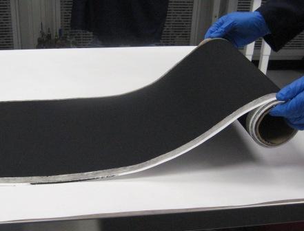
Buckypaper is a macroscopic aggregate of carbon nanotubes (CNT) which is ultrathin, electrically conducting and 10 times lighter than steel while still being 250 times stronger. The tough material can be folded, cut with scissors, like notebook paper. Composed of tube-shaped carbon molecules 50,000 times thinner than a human hair, Buckypaper possesses unique properties enabling it to conduct electricity like brass or steel and disperse heat like metal or silicon.
In the 1980s a carbon atom arrangement called Carbon 60, or Buckminsterfullerene, was discovered that turned out to be twice as hard as diamond. The pattern of carbon atom links was found to be identical with the basic polyhedron that R. The flat-sheet hexagonal form of carbon could wrap around itself to create long hollow tubes. These nanotubes have a tensile strength 40 times greater than that of the carbon fibers currently used in aircraft. In 1985, a team of scientists at Rice University, while conducting an experiment examining how stars produce carbon serendipitously discovered a ball of 60 carbon atoms, which scientists named "Buckyballs." The naming came from the buckminsterfullerene, the 60 carbon fullerene. Buckypaper is the brainchild of professor Ben Wang, an industrial engineer at Florida State University who discovered the carbon nanotubes of Buckyballs would stick together and could be produced into a small film.
Buckypaper is created from carbon nanotubes, which can be magnetically aligned during fabrication. Carbon nanotubes are suspended in water. Then the suspension is filtered the onto a membrane support. After drying, the paper is removed from the support, leaving a free-standing paper.
Buckypaper can be implicated in military vehicles to make them lighter and stronger, to make transporting these vehicles to trouble areas faster and more efficient. Also, buckypaper in the future is predicted to be applicable as a large-scale electron-field emitter for flat-panel displays, as a thermal conductor for superefficient heat sinks and as high-current protective film for the exteriors of airplanes. Such film would allow lightning strikes to flow around a plane and dissipate without damaging it.                                                                                                                                              

Buckypaper Applications:
Buckypaper is used in airplane industry.
Buckypaper is used in military armor plating.
Buckypaper is used in biological tissues.
Buckypaper is used in LCD (computer and TV) screens.
Buckypaper is used in sensor technology.

Comments

Popular posts from this blog

Molybdenum Trioxide Nanoparticles/Nanopowder and Applications

General Information about Molybdenum Trioxide                                                     Molybdenum trioxide is chemical compound with the formula MoO3. Its chief application is as an oxidation catalyst and as a raw material for the production of molybdenum metal.  Molybdenum Trioxide  is a very light blue powder. Molybdenum Trioxide Nanoparticles/Nanopowder and Their Applications                                                    Like many  nanoparticles/nanopowder , Molybdenum Trioxide nanoparticles/nanopowder are used as catalysts. These catalysis reactions include hydrogenation catalysis and cracking catalysis. Molybdenum Trioxide nanoparticles/  nanopowder are useful for...

Hydroxyapatite Nanopowders and Their Applications

Hydroxyapatite, is a naturally occurring mineral form of calcium apatite with the formula Ca 5 (PO 4 ) 3 (OH). Pure hydroxyapatite powder is white. Naturally occurring apatites can, however, also have brown, yellow, or green colorations, comparable to the discolorations of dental fluorosis. Hydroxyapatite Nanopowder/Nanoparticles (50 nm, 99.95+%)  has been widely used as a biocompatible ceramic in many areas of medicine, but mainly for contact with bone tissue, due to its resemblance to mineral bone. In mammals, the skeleton presents a carbonated and partially substituted apatite, based on nanocrystal aggregates, and associated with collagen, building up 3-D structures present in various bone tissue conformations like trabecular or cancellous bone. There has been growing interest in developing bioactive synthetic ceramics that could closely mimic natural apatite characteristics. As mentioned before,  Hydroxyapatite Nanopowder  is the main inorganic constituent of bon...

Rundown about Silicon Oxide Wafer

The main insulating material used in micro-technology is Silicon Dioxide, which in chemical symbols is written as SiO2. In semiconductor technology, SiO2 thin film layers are mainly used as dielectric material film in transistors, capacitors (DRAM) or flash-memories. Silicon Oxide Wafers are produced using crystallization, solid state and other ultra-high purification processes such as sublimation. This process forms a cylindrical ingot, which is then sliced and polished to form wafers. Thermal oxide is a kind of "grown" oxide layer, compared to CVD deposited oxide layer, it has a higher uniformity, and higher dielectric strength, it is an excellent dielectric layer as an insulator . In most silicon- based devices, thermal oxide layer play an important role to pacify the silicon surface to act as doping barriers and as surface dielectrics. The simplest way to produce an insulating silicon oxide layers (SiO2) on silicon wafers is to oxidize silicon with oxygen, which ...