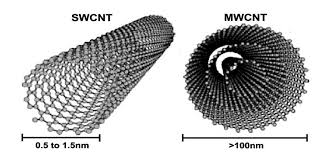
Progress of manufacturing technology of a cheaper and significantly more high-quality carbon nanotubes has caused an increased industrial applications for this outstandıng material. One of the applications, carbon nanotubes conductive films with metal, is an alternative technology for electronics that may easily replace oldfashioned traditional transparent conductive films, that tipically use indium tin oxide. Metallic nanoparticles/nanopowder decorated on carbon nanotubes highly conductive films show a cheap and efficient option for the applications in touch screens and the replacement of the ITO film because of their interesting properties of electrical conductivity, mechanical property, chemical inertness, and other unique properties, which may not be accessible by their individual components. However, a great challenge that always remains is to develop effective ways to prepare junctions between metallic nanoparticles/nanopowder and carbon nanotubes highly conductive films for the improvement of high-energy barriers, high contact resistances, and weak interactions which could lead to the formation of poor conducting pathways and result in the CNT-based devices with low mechanical flexibility.
Carbon nanotubes highly conductive films are of great importance to a number of applications such as optical and electronic devices. In an example application, the carbon nanotubes highly conductive films are used to construct an electric field-activated optical modulator, which constitutes an optical analog to the nanotube-based field effect transistor. The carbon nanotubes highly conductive films could make manufacturing LCD screens faster and cheaper. The carbon nanotubes highly conductive films could enhance the life of touch panels used in ATM screens and supermarket kiosks. The carbon nanotubes highly conductive films might also pave the way for flexible thin-film solar cells and bright, roll-up color displays. Those displays could be used in cell phones, billboards, and electronic books and magazines.
In traditional applications, the carbon nanotubes highly conductive films would replace the indium tin oxide (ITO) coatings that are currently used as transparent electrodes. ITO cracks easily and is a more expensive material. Touch panels–which are particularly susceptible to the brittleness of ITO–will be the first market that the company will target. Many display manufacturers are working on products using the carbon nanotubes highly conductive films. In October, Samsung demonstrated the first prototype of a 14.3-inch color electronic paper device made with the carbon nanotubes highly conductive films.
Carbon nanotubes highly conductive films with metal applications:
Carbon nanotubes highly conductive films are used in electronic screens and displays.
Carbon nanotubes highly conductive films are used in solar cells.
Carbon nanotubes highly conductive films are used in replacement of ITO coatings.
Carbon nanotubes highly conductive films are used in optical devices.
Comments
Post a Comment