
Terbium Characteristics and General Information

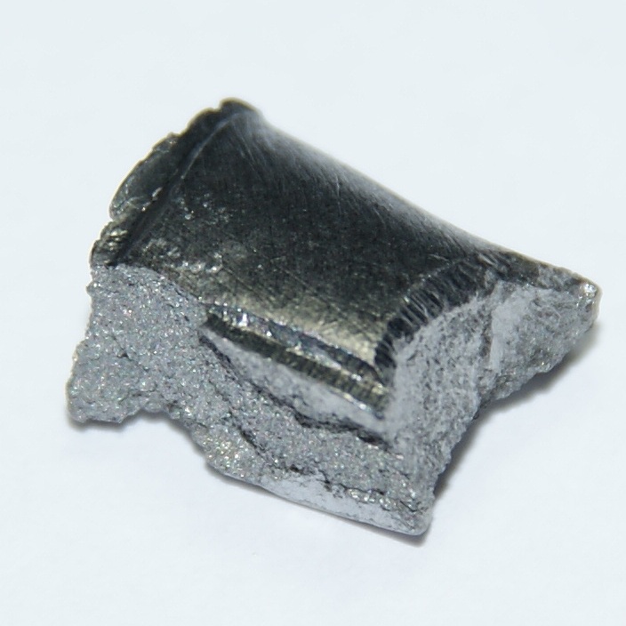
Terbium(Tb) is the one of the lanthanide element with an atomic number 63. Terbium is a silvery white earth metal that is malleable, ductile and soft enough to be cut with a knife. Terbium is an electropositive metal that reacts with water producing hydrogen gas. Terbium is never found as pure element in nature. However, terbium is found as component of many minerals like cerite, gadolinite, monazite, xenotime nad euxenite. Terbium was discovered by Swedish chemist Carl Gustaf Mosander as a separate elemental compound in 1843. Terbium was named after the village of Ytterby in Sweden as yttrium metal. Terbium was not purified until ion exchange technique was found. Most of terbium supply is used in green phosphorous. Nowadays, the richest commercial sources of terbium are the ion-adsorption clays of southern China. Only small amounts of terbium occur in bastnasite and monazite. Due to terbium’s rareness and its expensive prices, it has few commercial uses.

Applications of Terbium:
Terbium is used as a dopant in calcium fluoride, calcium tungstate and strontium molybdate. These 3 materials are used in solid-state devices and as crystal stabilizer of fuel cells which operate at elevated temperatures
Terbium is used in alloys and in the production of electronic devices.
Terbium is used in actuators, in naval sonar systems, sensors, in the SoundBug device and other magnetomechanical devices
Terbium is used as a probe in biochemistry, where it resembles calcium in its behavior
Terbium is used to detect endospores, as it acts as an assay of dipicolinic acid based on photoluminescence
Terbium is used in laser and semiconductor devices
Terbium is used in color phosphorous in lighting applications such as trichromatic lighting and in color TV tubes. It also makes the green color on Blackberry or other high definition screen
Terbium is used to make terbium-iron alloy which is needed to provide metallic films for magneto-optic recording of data
Terbium is used to make a magnet with neodymium and dysprosium that is base of electric motors of hybrid car engines and all other electric motors

Comments

Popular posts from this blog

Molybdenum Trioxide Nanoparticles/Nanopowder and Applications

General Information about Molybdenum Trioxide                                                     Molybdenum trioxide is chemical compound with the formula MoO3. Its chief application is as an oxidation catalyst and as a raw material for the production of molybdenum metal.  Molybdenum Trioxide  is a very light blue powder. Molybdenum Trioxide Nanoparticles/Nanopowder and Their Applications                                                    Like many  nanoparticles/nanopowder , Molybdenum Trioxide nanoparticles/nanopowder are used as catalysts. These catalysis reactions include hydrogenation catalysis and cracking catalysis. Molybdenum Trioxide nanoparticles/  nanopowder are useful for...

Rundown about Silicon Oxide Wafer

The main insulating material used in micro-technology is Silicon Dioxide, which in chemical symbols is written as SiO2. In semiconductor technology, SiO2 thin film layers are mainly used as dielectric material film in transistors, capacitors (DRAM) or flash-memories. Silicon Oxide Wafers are produced using crystallization, solid state and other ultra-high purification processes such as sublimation. This process forms a cylindrical ingot, which is then sliced and polished to form wafers. Thermal oxide is a kind of "grown" oxide layer, compared to CVD deposited oxide layer, it has a higher uniformity, and higher dielectric strength, it is an excellent dielectric layer as an insulator . In most silicon- based devices, thermal oxide layer play an important role to pacify the silicon surface to act as doping barriers and as surface dielectrics. The simplest way to produce an insulating silicon oxide layers (SiO2) on silicon wafers is to oxidize silicon with oxygen, which ...

New Way of Deaf-Mute Communication with 3D Graphene

Image retrieved from: http://blogs.rsc.org/cc/2016/09/01/3d-graphene-adds-dimension-to-deaf%E2%80%93mute-communication/ Chinese scientists have developed wearable electronic device with conductive 3D graphene structure to translate sign language into written text. This technology can be applied by injecting graphene ink from a syringe under printed electronic field. For medical field, such as adhesive patches which determine heart, brain signal and neural activity, wearable and bio-integrated medical devices are very important. Due to noticeable properties of cast graphene, for example a 2D honeycomb lattice, excellent mechanical and electrical behaviors, Graphene has an important material in warble technology. However, it is difficult to preserve advantages of Graphene material in a 3D material which has an information about forces from every angle. Yanlin Song  and co-workers at the University of the Chinese Academy of Sciences, Beijing, and Shenyang Jianzhu University...