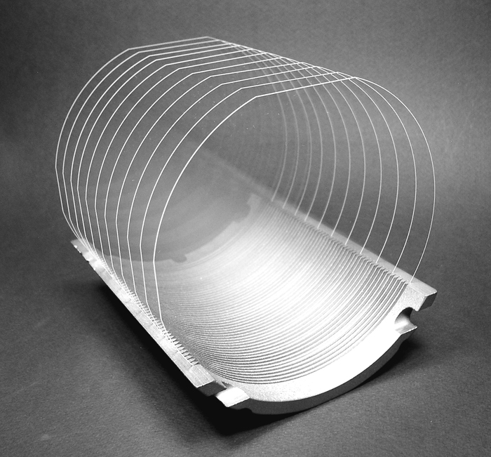
Borosilicate glass wafers are widely used for the process of anodic bonding of silicon with glass, so that the silicon’s thermal expansion is alike to these materials. Borosilicate glass wafers were developed for thin film electronic circuits, which require an extremely smooth surface with special electrical properties. The general application of thin and ultrathin Borosilicate glass wafers is an electronic packaging of optoelectronic conductors.
Borosilicate glass wafers are preferred in many industries, e.g. research and biomedical industry, thanks to its affordability. Borosilicate glass wafers, in case of an explosion to high temperatures manages to remain clear and solid. The production applies the coating of Indium Tin Oxide onto the surface, that is transparent in a visible spectrum which reflects the infrared spectrum back at the light source. This coating is also electrically conductive (~50 ohms/square). Such technology is required for the protection of the insides of lenses, cameras and film in projectors from heat of the light sources.
Borosilicate glass wafers are the base for a large number of MEMS applications and wide range of micro-optical Applications.
- Borosilicate glass wafers are used in CMOS (complementary metal oxide semiconductor) image sensors.
- Borosilicate glass wafers are used in Microfluidics (e.g. for medical analysis, drug testing or dosing)
- Borosilicate glass wafers are used in CCD (charges coupled device) image sensors
- Borosilicate glass wafers are used in Lens systems
- Borosilicate glass wafers are used in Biochips (e.g. arrays for DNA analysis)
- Borosilicate glass wafers are used in Pressure Sensors
- Borosilicate glass wafers are used in Carrier Wafers
- Borosilicate glass wafers are used in Microlens Arrays
- Borosilicate glass wafers are used in Wafer level chip size packaging
- Borosilicate glass wafers are used in Diffractive Optics
Comments
Post a Comment