
General Information About Ytterbium

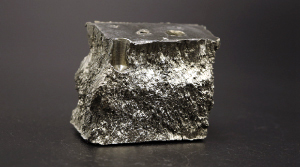
Ytterbium(Yb) is the one of the lanthanide elements with an atomic number 70. Ytterbium is a bright, soft, silvery-white rare earth metal. Malleability and ductility are also two properties of ytterbium metal. Due to ytterbium is a little electropositive element, it slowly reacts water resulting in ytterbium hydroxide. Ytterbium reacts with all halogens. +2 oxidation state is the basis of the relative stability, but ytterbium, as other rare earth metals, usually has +3 oxidation state in most compounds. The discovery of ytterbium was made in Geneva, Switzerland by Swiss chemist Jean Charles Galissard de Marginac in 1878. The name comes from the name of Swiss village Ytterby. 1937 is year when ytterbium metal was purified by Klemm and Bonner by heating ytterbium chloride with potassium. In 1953 the pure ytterbium was produce at th Ames laboratory from which both physical and chemical properties could be measured. The commercial source of ytterbium is monazite mineral. However, ytterbium also exists in other minerals as well. Like other rare earth metals ytterbium is separated by ion-exchange and solvent extraction techniques. The price of ytterbium in 1998 was about $1000 per kilogram.
Applications of Ytterbium:
Ytterbium is used as radiation source in portable X-ray machines which emits gamma rays which could pass through soft tissues of the body. However, this gamma ray is blocked by dense materials like bone.
Ytterbium is used in nuclear medicine
Ytterbium is used in ticking clocks since these clocks hold the record for stability
Ytterbium is used as dopant because it improves the grain strength and refinement. In addition, it may improve some mechanical properties of stainless steel
Ytterbium is used to mix with other metal resulting in alloys which are used in dentistry
Ytterbium is used as dopant in solid state lasers and double clad fiber lasers, since ytterbium has long lifetimes, ability to generate short pulses and is highly efficient
Ytterbium is used when there is need to increase electrical resistivity
https://nanografi.com/rare-earth-materials/yb-ytterbium-powder-325-mesh-99-5/

Comments

Popular posts from this blog

Molybdenum Trioxide Nanoparticles/Nanopowder and Applications

General Information about Molybdenum Trioxide                                                     Molybdenum trioxide is chemical compound with the formula MoO3. Its chief application is as an oxidation catalyst and as a raw material for the production of molybdenum metal.  Molybdenum Trioxide  is a very light blue powder. Molybdenum Trioxide Nanoparticles/Nanopowder and Their Applications                                                    Like many  nanoparticles/nanopowder , Molybdenum Trioxide nanoparticles/nanopowder are used as catalysts. These catalysis reactions include hydrogenation catalysis and cracking catalysis. Molybdenum Trioxide nanoparticles/  nanopowder are useful for...

Rundown about Silicon Oxide Wafer

The main insulating material used in micro-technology is Silicon Dioxide, which in chemical symbols is written as SiO2. In semiconductor technology, SiO2 thin film layers are mainly used as dielectric material film in transistors, capacitors (DRAM) or flash-memories. Silicon Oxide Wafers are produced using crystallization, solid state and other ultra-high purification processes such as sublimation. This process forms a cylindrical ingot, which is then sliced and polished to form wafers. Thermal oxide is a kind of "grown" oxide layer, compared to CVD deposited oxide layer, it has a higher uniformity, and higher dielectric strength, it is an excellent dielectric layer as an insulator . In most silicon- based devices, thermal oxide layer play an important role to pacify the silicon surface to act as doping barriers and as surface dielectrics. The simplest way to produce an insulating silicon oxide layers (SiO2) on silicon wafers is to oxidize silicon with oxygen, which ...

New Way of Deaf-Mute Communication with 3D Graphene

Image retrieved from: http://blogs.rsc.org/cc/2016/09/01/3d-graphene-adds-dimension-to-deaf%E2%80%93mute-communication/ Chinese scientists have developed wearable electronic device with conductive 3D graphene structure to translate sign language into written text. This technology can be applied by injecting graphene ink from a syringe under printed electronic field. For medical field, such as adhesive patches which determine heart, brain signal and neural activity, wearable and bio-integrated medical devices are very important. Due to noticeable properties of cast graphene, for example a 2D honeycomb lattice, excellent mechanical and electrical behaviors, Graphene has an important material in warble technology. However, it is difficult to preserve advantages of Graphene material in a 3D material which has an information about forces from every angle. Yanlin Song  and co-workers at the University of the Chinese Academy of Sciences, Beijing, and Shenyang Jianzhu University...