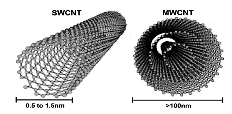
Carbon nanotubes called cylindrical nanostructured allotropes of carbon with a one atom thick, and the diameter depends on the purpose of applications. Carbon nanotubes have extraordinary properties in mechanics and electrics, especially stiffness and strength. Its qualities make carbon nanotubes valuable for nanotechnology, electronics, optics, and fields of material science. Number of walls classify the carbon nanotubes as single-walled, double-walled, triple walled, and multi walled. Multi-walled means there are multiple nanotubes inside the other nanotubes with different diameters, and there is nothing inside the nanotubes in the case of single-walled nanotube.
Figure 1: Schematic representation of Single Walled Carbon Nanotube (SWCNT) and Multi Walled Carbon Nanotube (MWCNT)
https://www.researchgate.net/publication/319966218_Carbon_nanotube_buckypaper_reinforced_polymer_composites_A_review/figures?lo=1
Single-Walled Carbon Nanotubes (SWCNT) have unique properties. In terms of mechanics, they are 100 times more tensile than steel at 1/16th weight, but in practice, due to defects, half of the predicted values are measured. From the aspect of electrical properties, Single-walled carbon nanotubes has current carrying capacity of 109amp/cm2 which is higher than those of gold, copper, and semiconductors. In addition, they have unique optical absorption and fluorescence response depending on the chirality of the nanotubes. That makes excellent to replace indium tin oxide as the transparent conductor since the transparency of coating formed with single-walled carbon nanotubes are high in the visible and IR regions of the spectrum. Also, thermal conductivity of it can be compared to that of diamond.
Single-Walled Carbon Nanotubes (SWCNT) have unique properties. In terms of mechanics, they are 100 times more tensile than steel at 1/16th weight, but in practice, due to defects, half of the predicted values are measured. From the aspect of electrical properties, Single-walled carbon nanotubes has current carrying capacity of 109amp/cm2 which is higher than those of gold, copper, and semiconductors. In addition, they have unique optical absorption and fluorescence response depending on the chirality of the nanotubes. That makes excellent to replace indium tin oxide as the transparent conductor since the transparency of coating formed with single-walled carbon nanotubes are high in the visible and IR regions of the spectrum. Also, thermal conductivity of it can be compared to that of diamond.
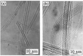
Figure 2: Tem images a, showing a 5 nm projected diameter carbon nanotube that is bent like letter “z” but still not broken; b, showing SWNT bundles with some wavy parts.
Single-Walled Carbon Nanotubes have wide range of applications which are sensors, biomedical applications, thin film transistors, transparent electrodes, biomedical applications, field emissions, conductive composites, interconnects, battery electrodes, drug delivery, gas storage, super capacitors, fibers, hard coatings, bio-scaffolds, strong composites, and actuators.
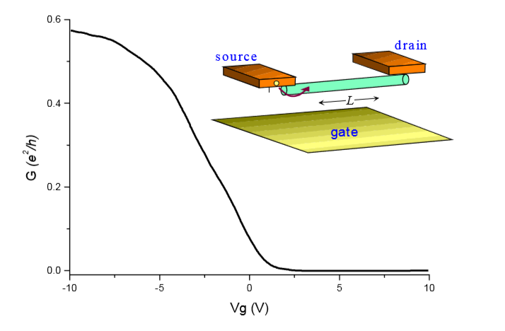
Figure 3: Conductance G vs. gate voltage Vg of a p-type semiconducting SWNT field effect transistor. The device geometry is shown schematically in the inset.
Paul L McEuen, Michael Fuhrer, Hongkun Park, Single Walled Carbon Nanotube Electronics, 2002.
As an example research, Dr. Benjamin FLAVEL and his team solved the issue of reductions in efficiency caused by the short exciton diffusion length of approximately 5-10 nm in organic solar cells with using single-walled carbon nanotubes which have estimated exciton diffusion length of 0.1-1 µm. Another example is that, single walled carbon nanotube has semiconducting behavior, as seen in figure 3, conductance is varied when the gate voltage applied to the conducting substrate. If Vg is negative, It conducts, otherwise, it turns off, so it behave like p-type MOSFET with replacing Si with single-walled carbon nanotube.
Although carbon nanotubes are discovered at 1991, there is a huge advance in research from photonics to biomedical applications. Its properties make it very interesting material. Therefore, In the future, Its applications will be enhanced, and increasing the production efficiency, it will replace most of the materials with lots of advantages.
Comments
Post a Comment