
Dysprosium Oxide Nanoparticles

Dy2O3(Dysprosium Oxide) Nanoparticles and Applications of Dysprosium Oxide Nanopowder
What is Dysprosium Oxide?
Dysprosium Oxide (Dy2O3) is a chemical compound which consists of a rare metal Dysprosium and Oxygen. It is a solid in room temperature and has a very high melting point which is 2408 °C.
Uses and Properties of Dysprosium Oxide
Dysprosium Oxide is suitable for ceramics, glass, phosphors, lasers and metal halide lamps applications. This compound is used in electronics industry as an antireflection coating in photoelectric devices. Because of dysprosium's high thermal-neutron absorption cross-section, Dysprosium-Oxide–Nickel cermets are used in neutron-absorbing control rods in nuclear reactors. Dysprosium and its compounds are highly susceptible to magnetization, they are employed in various data-storage applications, such as in hard disks.
Why Nanoparticles are Important?
Nanoparticles are particles between 1 and 100 nanometers in size. Interest in nanoparticles is motivated by their interesting electronic, optical, magnetic, mechanical, and chemical properties, which are totally different from those of their bulk counterparts.
An image of dysprosium oxide nanoparticles, obtaine
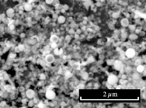
d with a scanning electron microscope Quanta 600 FEG*
Application Areas of Dysprosium Oxide Nanoparticles
There are many applications that Dysprosium oxide nanoparticles can be used. For instance Dysprosium oxide nanoparticles can be used as a high surface area for catalytic compounds. For fluorescent materials Dysprosium Oxide nanoparticles are dopants. Dysprosium oxide nanoparticles are also used in measurement of neutron energy-spectrum. For glass material in laser-based and optical devices with a Faraday Rotation affect Dysprosium oxide nanoparticles can be used.
Technical Properties of our Dy2O3(Dysprosium Oxide) Nanoparticles, 28nm, High Purity 99.95+% product
Purity %99.95+
Colorwhite
AVERAGE PARTICLE SIZE (nm):28
Morphologyspherical
SPECIFIC SURFACE AREA (m2/g):>30
Bulk Density (g/cm3)0,5
True Density (g/cm3)8
You may find Dy2O3(Dysprosium Oxide) Nanoparticles, 28nm, High Purity 99.95+% by clicking the link below:
Technical Properties of our Dysprosium Oxide, 99.99%325 mesh product
Purity %
99.99
Colorwhite
SIZE (mesh):325
You may find Dysprosium Oxide, 99.99%325 mesh by clicking the link below:
https://nanografi.com/rare-earth-materials/dysprosium-oxide-99-99-325-mesh/
*https://www.researchgate.net/figure/An-image-of-dysprosium-oxide-nanoparticles-obtained-with-a-scanning-electron-microscope_fig2_318678438

Comments

Popular posts from this blog

Molybdenum Trioxide Nanoparticles/Nanopowder and Applications

General Information about Molybdenum Trioxide                                                     Molybdenum trioxide is chemical compound with the formula MoO3. Its chief application is as an oxidation catalyst and as a raw material for the production of molybdenum metal.  Molybdenum Trioxide  is a very light blue powder. Molybdenum Trioxide Nanoparticles/Nanopowder and Their Applications                                                    Like many  nanoparticles/nanopowder , Molybdenum Trioxide nanoparticles/nanopowder are used as catalysts. These catalysis reactions include hydrogenation catalysis and cracking catalysis. Molybdenum Trioxide nanoparticles/  nanopowder are useful for...

Rundown about Silicon Oxide Wafer

The main insulating material used in micro-technology is Silicon Dioxide, which in chemical symbols is written as SiO2. In semiconductor technology, SiO2 thin film layers are mainly used as dielectric material film in transistors, capacitors (DRAM) or flash-memories. Silicon Oxide Wafers are produced using crystallization, solid state and other ultra-high purification processes such as sublimation. This process forms a cylindrical ingot, which is then sliced and polished to form wafers. Thermal oxide is a kind of "grown" oxide layer, compared to CVD deposited oxide layer, it has a higher uniformity, and higher dielectric strength, it is an excellent dielectric layer as an insulator . In most silicon- based devices, thermal oxide layer play an important role to pacify the silicon surface to act as doping barriers and as surface dielectrics. The simplest way to produce an insulating silicon oxide layers (SiO2) on silicon wafers is to oxidize silicon with oxygen, which ...

New Way of Deaf-Mute Communication with 3D Graphene

Image retrieved from: http://blogs.rsc.org/cc/2016/09/01/3d-graphene-adds-dimension-to-deaf%E2%80%93mute-communication/ Chinese scientists have developed wearable electronic device with conductive 3D graphene structure to translate sign language into written text. This technology can be applied by injecting graphene ink from a syringe under printed electronic field. For medical field, such as adhesive patches which determine heart, brain signal and neural activity, wearable and bio-integrated medical devices are very important. Due to noticeable properties of cast graphene, for example a 2D honeycomb lattice, excellent mechanical and electrical behaviors, Graphene has an important material in warble technology. However, it is difficult to preserve advantages of Graphene material in a 3D material which has an information about forces from every angle. Yanlin Song  and co-workers at the University of the Chinese Academy of Sciences, Beijing, and Shenyang Jianzhu University...