Copper Nanoparticles and Applications of Copper Nanopowders
Information about Copper
Copper is a chemical element with symbol Cu and atomic number 29. It is a soft, malleable, and ductile metal with very high thermal and electrical conductivity. A freshly exposed surface of pure copper has a reddish-orange color. Copper is used as a conductor of heat and electricity, as a building material, and as a constituent of various metal alloys, such as sterling silver used in jewelry, cupronickel used to make marine hardware and coins, and constantan used in strain gauges and thermocouples for temperature measurement.
Copper Nanoparticles*
Nanoparticles of Copper and Application Areas
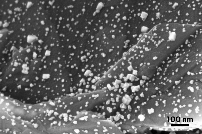
Copper Nanoparticles display unique characteristics including catalytic and antifungal/antibacterial activities that are not observed in commercial copper. Copper Nanoparticles demonstrate a very strong catalytic activity, a property that can be attributed to their large catalytic surface area. With the small size and great porosity, the nanoparticles can achieve a higher reaction yield and a shorter reaction time when utilized as reagents in organic and organometallic synthesis. Copper Nanoparticles with great catalytic activities can be applied to biosensors and electrochemical sensors. Redox reactions utilized in those sensors are generally irreversible and also require high overpotentials (more energy) to run. In fact, the nanoparticles have the ability to make the redox reactions reversible and to lower the overpotentials when applied to the sensors. Copper nanoparticles that are extremely small and have a high surface to volume ratio can also serve as antifungal/antibacterial agents. The antimicrobial activity is induced by their close interaction with microbial membranes and their metal ions released in solutions. Copper Nanopowders can be used as a replacement for more expensive metals, because Copper Nanopowders are ideal for reducing production costs, and find wide usage in microelectronic processes, conductive pastes, and as nanometal lubricant and sintering additives.
Technical Properties of Our Cu(Copper) Nanoparticles, 99.95%, 35 nm, metal basis Product
| Bulk Density (g/cm3): | 0,19 |
| True Density (g/cm3): | 8,9 |
| Color: | warm copper brown |
| Shape: | spherical |
| Crystal Structure: | cubic |
| AVERAGE PARTICLE SIZE (nm): | 35 |
| SPECIFIC SURFACE AREA (m2/g): | 11,0-15,0 |
You may find Cu(Copper) Nanoparticles, 99.95%, 35 nm, metal basis from the link given below:
Technical Properties of our Cu(Copper) Nanoparticles, 99.95%, 80nm, metal basis product
| Bulk Density (g/cm3): | 0,22 |
| True Density (g/cm3): | 8,9 |
| Color: | warm copper brown |
| Shape: | spherical |
| Crystal Structure: | cubic |
| AVERAGE PARTICLE SIZE (nm): | 100 |
| SPECIFIC SURFACE AREA (m2/g): | 5,0-5,8 |
You may find Cu(Copper) Nanoparticles, 99.95%, 80nm, metal basis from the link given below:
Technical Properties of our Cu(Copper) Nanoparticles 99.95%, 65nm, metal basis product
| Bulk Density (g/cm3): | 0,22 |
| True Density (g/cm3): | 8,9 |
| Color: | warm copper brown |
| Shape: | spherical |
| Crystal Structure: | cubic |
| AVERAGE PARTICLE SIZE (nm): | 65 |
| SPECIFIC SURFACE AREA (m2/g): | 6,5-7,5 |
You may find Cu(Copper) Nanoparticles 99.95%, 65nm, metal basis from the link given below:
Technical Properties of our Cu(Copper) Nanoparticles Partially Passivated,99.85%, 22 nm product
| Cu Purity (%): | ≥99,8 |
| Bulk Density (g/cm3): | 0,2-0,4 |
| True Density (g/cm3): | 8,9 |
| Color: | dark brown |
| Shape: | spherical |
| Crystal Structure: | cubic |
| AVERAGE PARTICLE SIZE (nm): | 25 |
| SPECIFIC SURFACE AREA (m2/g): | 35,0-55,0 |
You may find Cu(Copper) Nanoparticles Partially Passivated,99.85%, 22 nm from the link given below:
Technical Properties of our Cu(Copper) Nanoparticles, 99.95%, 570 nm, metal basis product
| Bulk Density (g/cm3): | 0,7-1,1 |
| True Density (g/cm3): | 8,9 |
| Color: | reddish brown |
| Shape: | spherical |
| Crystal Structure: | cubic |
| AVERAGE PARTICLE SIZE (nm): | 570 |
| SPECIFIC SURFACE AREA (m2/g): | 4,6 |
You may find Cu(Copper) Nanoparticles, 99.95%, 570 nm, metal basis from the link given below:
Technical Properties of our Cu(Copper) Nanoparticles, 99.95%, 80-240 nm, metal basis product
| Bulk Density (g/cm3): | 0,25 |
| True Density (g/cm3): | 8,9 |
| Color: | reddish brown |
| Shape: | spherical |
| Crystal Structure: | cubic |
| AVERAGE PARTICLE SIZE (nm): | 80-240 |
| SPECIFIC SURFACE AREA (m2/g): | 4,6 |
You may find Cu(Copper) Nanoparticles, 99.95%, 80-240 nm, metal basis from the link given below:
Technical Properties of our Cu(Copper) Nanoparticles 99.95%, 780 nm, metal basis product
| True Density (g/cm3): | 8,9 |
| Color: | reddish brown |
| Shape: | spherical-rectangular |
| Crystal Structure: | cubic |
| AVERAGE PARTICLE SIZE (nm): | 800 |
| SPECIFIC SURFACE AREA (m2/g): | 1,8 |
You may find Cu(Copper) Nanoparticles 99.95%, 780 nm, metal basisfrom the link given below:
Technical Properties of our Cu(Copper) Nanoparticles Carbon Coated, 99.85%, 22 nm product
| Cu Purity (%): | ≥99,85 |
| Bulk Density (g/cm3): | 0,2-0,4 |
| True Density (g/cm3): | 8,9 |
| Color: | black |
| Shape: | spherical |
| Crystal Structure: | cubic |
| AVERAGE PARTICLE SIZE (nm): | 22 |
| SPECIFIC SURFACE AREA (m2/g): | 35,0-55,0 |
You may find Cu(Copper) Nanoparticles Carbon Coated, 99.85%, 22 nmfrom the link given below:
Comments
Post a Comment