Boron Nitride Nanoparticles and Boron Nitride Nanopowder Applications
Boron nitride, consists of Boron and Nitrogen, is a heat and chemically resistant chemical compound with the chemical formula BN. Because of excellent thermal and chemical stability, boron nitride ceramics are traditionally used as parts of high-temperature equipment.
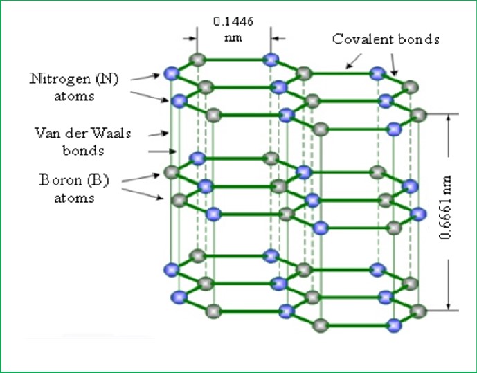
Boron Nitride has four different structures that differ in the arrangement of boron and nitrogen atoms, but the most stable crystalline form of this compound is hexagonal form.
Schematic of hexagonal boron nitride (h-BN) structure*
Nanoparticles of Boron Nitride and Application Areas
The Nanoparticles of Boron Nitride are extremely fine powder. Because of its hardness, thermal and electrical properties, there are many areas that Boron Nitride Nanoparticles can be useful. It is not hard to say that Boron Nitride is an essential compound for industrial usage. Boron Nitride Nanoparticles have applications in subsurface investigation, oil drilling, and high-speed cutting tools. Boron Nitride Nanoparticles are used as a metal forming and metal drawing lubricant release agent. These nanoparticles can be pressed into different shapes and used as high voltage, high temperature, insulation and cooling components. Boron Nitride Nanoparticles are useful to be used in transistors, plasma arc's insulators, high-voltage high frequency electricity, semi-conducting solid phase admixtures, high-frequency induction furnace materials, atom reactor's structure materials, preventing neutron radiation's packing materials, automatic welding high-temperature coating, radar antenna's mediums, radar's pass box, and rocket engine's components. The other usage area of Boron Nitride Nanoparticles is being catalyst for high temperature and high-pressure treatments. It should be well known that Boron Nitride Nanoparticles used as a composite for ceramics, as thermally conductive filler for polymers, and as high temperature lubricant. Since Boron Nitride Nanoparticles can be used in heat shielding materials, it is used in the aerospace industry.
So, it can be said that Boron Nitride Nanoparticles have excellent performance, wide application and great potential, and play an important role in many technical fields.
Technical Properties of Our BN Nanoparticles(Boron Nitride) 99.7%, 790nm, Hexagonal Product
| Purity (%) | 99.7 |
| AVERAGE PARTICLE SIZE (nm): | 790 |
| True Density (g/cm3) | .2,3 |
You may contact with us for your needs of BN Nanoparticles(Boron Nitride) 99.7%, 790nm, Hexagonal by clicking the link below:
Technical Properties of Our BN Nanoparticles(Boron Nitride) 99.85+%, 65-75nm, Hexagonal Product
| Purity (%) | 99.85 |
| AVERAGE PARTICLE SIZE (nm): | 65-75 |
| True Density (g/cm3) | .2,3 |
You may contact with us for your needs of BN Nanoparticles(Boron Nitride) 99.85+%, 65-75nm, Hexagonalby clicking the link below:
https://nanografi.com/nanoparticles/bn-nanoparticles-boron-nitride-99-85-65-75nm-hexagonal/
*https://www.researchgate.net/figure/Schematic-of-hexagonal-boron-nitride-h-BN-structure_fig1_258712674
Comments
Post a Comment